Software Development Environment
The SDE used to develop software is Keil MDK-ARM. This is a Microcontroller Development Kit with support for Cortex-M, Cortex-R4, ARM7 and ARM9 devices. From this development kit we’ll use μVision as an integrated Development Environment (IDE) and debugger. This debugger can communicate directly with the ST-Link on the target board.
The software can be downloaded for free from the Keil website: http://www.keil.com/arm/mdk.asp. Two of the limitations of this free version are that it can generate ‘only’ 32 kB binaries and it does not generate list files.
- Download and install Keil MDK-ARM.
When running μVision for the first time, the ‘Pack Installer’ starts automatically. This is a utility for installing, updating and removing Software Packs. These packs contain vendor specific files and/or examples. If it does not start automatically, open it by clicking .

Be sure to at least install the following pack: Keil::STM32F0xx_DFP

ST-LINK/V2 drivers
The development board has an integrated programmer debugger called ST-LINK/V2. Keil MDK-ARM does not install the drivers, so be sure to install the drivers for your operating system from this website:
Verify software installation
This lesson comes with a ZIP file containing example code. We will use this ZIP file to verify the installation of the software.
- Download this ZIP file here:
https://docs.google.com/file/d/0B-H5UhFxO23xRTY2cjVyLXZVQTA/edit?usp=sharing
- Unzip this file to any directory. By default, MDK-ARM projects are placed in the folder c:\keil\ARM
- Start μVision by double clicking the file blinky.uvprojx
- Build the project by pressing F7 or
The Build Output should look like this: - Connect the STM32F0-Discovery board to your PC/laptop.
- Program the microcontroller by pressing the load button or from the menu Flash -> Download

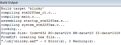

If everything is correctly installed, the Build Output windows displays the following message and the green and blue LED’s start blinking:

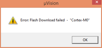
If the following error occurs, the programming algorithm is probably missing:
Do the following to solve this problem:
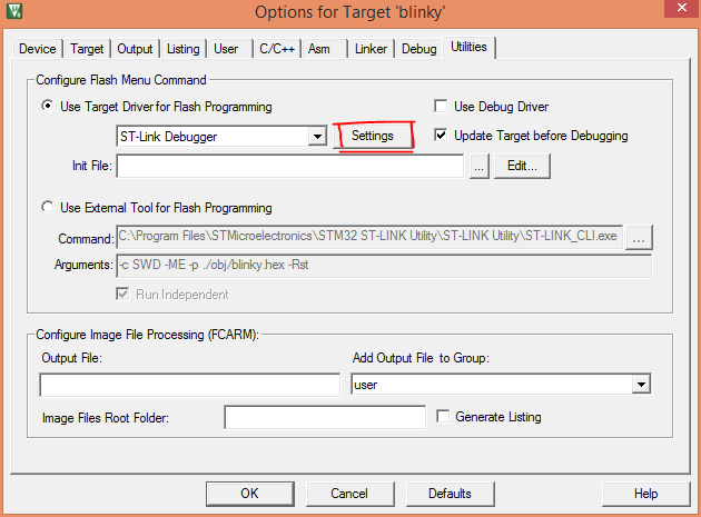
- Open the options:
Project -> Options for target ‘blinky’... (or or ALT+F7) - Select the Utilities tab and click settings:
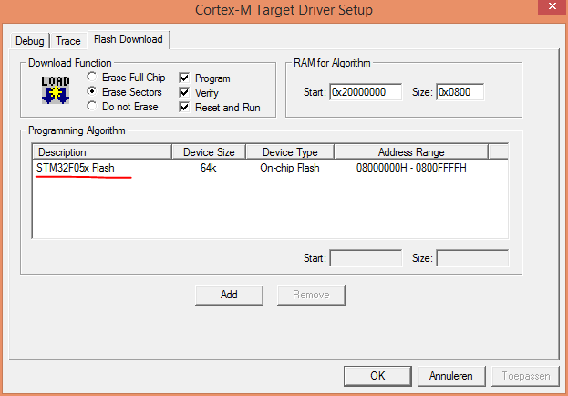
- Click Add to add the programming algorithm for the STM32F05x 64k flash.

New projects
The microcontroller used during these lessons is the STM32F051R8T6 from ST Microelectronics. To help getting started quickly a discovery board is used. All information about this STM32F0DISCOVERY board is listed here:
The User Manual UM1523 describes in more detail how to use the SDE. Chapter 1 describes how to get started and chapter 6 discusses how to use the Keil MDK-ARM. Study these chapters to get a basic understanding about the discovery board. These are also the chapters to study if you want to start a project from scratch. All lessons, however, have an example project associated with it where all MDK-ARM settings are already taken care of.
Project structure
Let’s have a look at one way to setup a project structure in Keil μVision. The structure used in these lessons will be similar to the example projects from STM used in later lessons.
- Open the μVision project associated with this lesson.
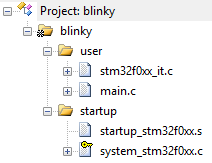
Take a look at the structure of the project files.
Note 1: Clicking the ‘+’ sign of a source file reveals all dependent header files.
Note 2: A ‘yellow key’ overlayed on the icon means the file is read only.
Note 1: Clicking the ‘+’ sign of a source file reveals all dependent header files.
Note 2: A ‘yellow key’ overlayed on the icon means the file is read only.
There are two folders and four files. The first folder is called ‘user’. Users can add any file necessary to the project to this folder. This example project contains:
- stm32f0xx_it.c: Contains the implementation of the main ISR’s and is provided by STM.
- main.c: Contains the main entry point.
The second folder is called ‘startup’. It contains files that were provided by STM:
- startup_stm32f0xx.s: Performs initial microcontroller setup by:
- setting initial Stack Pointer
- setting initial Program Counter
- setting the vector table with the ISR addresses
- branches to SystemInit in the file system_stm32f0xx_it.c
- branches to main. - system_stm32f0xx.c: Performs system clock configuration.
Before getting into more detail of code implementation, let’s discuss the basics of General-Purpose Inputs/Outputs. Then we are able to use these to implement a ‘blinky’ application.
General-Purpose Inputs/Outputs
GPIO pins can be used as digital General-Purpose Input- or Output. By software, they can be configured as input (with or without pull-up or pull-down) or as output (with push-pull or open-drain).
The GPIO’s of the STM32F051R8T6 are described in chapter 9 of the Reference Manual RM0091. This document can be found on the STM32F0DISCOVERY website under the tab ‘Design Resources’.

On the right side is the I/O pin. Each pin has two protection diodes that protect the pin from over- and undervoltages, like Electro Static Discharge (ESD). One of the diodes will conduct when a positive or negative voltage is applied to the I/O pin protecting the internal Input- and Output drivers.
When configured as an input, a pull-up resistor or a pull-down resistor can be enabled (not both), so there is no need for external resistors.
Via a buffer (in this case a Schmitt trigger) the logic value on the I/O pin is written to the Input data register.
When configured as an output, by default the Output driver is configured as push-pull. In this case, both FET’s (P-MOS and N-MOS) are controlled, making sure the logic value on the I/O pin is always 1 (Vdd) or 0 (Vss).
When the Output driver is configured as Open drain, only the N-MOS FET is controlled, so effectively the drain of this FET becomes ‘open’. Writing a logic 1 in the Output data register will make this FET conduct so it acts like a closed switch. Writing a logic 0 will make this FET not conduct. Essentially an open drain output can only sink and not source current.
When the Output driver is configured as Open drain, only the N-MOS FET is controlled, so effectively the drain of this FET becomes ‘open’. Writing a logic 1 in the Output data register will make this FET conduct so it acts like a closed switch. Writing a logic 0 will make this FET not conduct. Essentially an open drain output can only sink and not source current.
- Open document RM0091 - STM32F05xxx advanced ARM-based 32-bit MCUs.
- Study chapter 9.
In the example project the file main.c has the following code:
#include "stm32f0xx.h"
void delay(const int d);
int main(void)
{
// GPIOC Periph clock enable
RCC->AHBENR |= RCC_AHBENR_GPIOCEN;
// PC8 and PC9 in output mode
GPIOC->MODER |= (GPIO_MODER_MODER8_0 | GPIO_MODER_MODER9_0) ;
// Push pull mode selected
GPIOC->OTYPER &= ~(GPIO_OTYPER_OT_8 | GPIO_OTYPER_OT_9) ;
// Maximum speed setting
GPIOC->OSPEEDR |= (GPIO_OSPEEDER_OSPEEDR8 | GPIO_OSPEEDER_OSPEEDR9);
// Pull-up and pull-down resistors disabled
GPIOC->PUPDR &= ~(GPIO_PUPDR_PUPDR8 | GPIO_PUPDR_PUPDR9);
while(1)
{
// Set PC9
GPIOC->BSRR = GPIO_BSRR_BS_9;
// Reset PC8
GPIOC->BSRR = GPIO_BSRR_BR_8;
// Delay ~ 1 sec.
delay(SystemCoreClock/8);
// Reset PC9
GPIOC->BSRR = GPIO_BSRR_BR_9;
// Set PC8
GPIOC->BSRR = GPIO_BSRR_BS_8;
// Delay ~ 1 sec.
delay(SystemCoreClock/8);
}
}
|
To understand this code, let’s have a look at the 11 registers associated with a GPIO port. These are listed and described in the Reference Manual RM0091 in paragraph 9.4.
Four registers are used for initial setup:
- GPIOC_MODER: configures the I/O mode (input, output, alternate function or analog) (MODE Register)
- GPIOC_OTYPER: configures the I/O output type to push-pull or open drain (Output TYPE Register)
- GPIOC_OSPEEDR: configures the I/O output speed (Output SPEED Register)
- GPIOC_PUPDR: configures the I/O pull-up or pull-down (Pull-Up Pull-Down Register)
Two registers are used to read/write all I/O pins from a port at once:
- GPIOC_IDR: contains the logic input value of I/O port C
- GPIOC_ODR: contains the logic output value for I/O port C
One register to individually set/reset I/O pins, which enables programmers to create atomic bit set/reset actions:
- GPIOC_BSRR: writing a logic 1 to bits 31:16 resets the corresponding pin, writing a logic 1 to bits 15:0 sets the corresponding pin
Three ‘special’ registers (that are kept in their reset value in the code example):
- GPIOC_LCKR: lock the configuration of the port bits
- GPIOC_AFRL: enable alternate pin functions (like USART, ISP, etc.)
- GPIOC_AFRH: enable alternate pin functions (like USART, ISP, etc.)
One register to individually reset I/O pins:
- GPIOC_BRR: writing a logic 1 to bits 15:0 resets the corresponding pin
These registers are so-called ‘mapped’ to the microcontrollers memory. This is also called the register map and the first part looks like this:

The header file stm32f0xx.h describes the entire register map of all peripherals, so programmers can use definitions instead of addresses. All peripherals are described with a structure, making the register maps available as a new data type. The structure for GPIO peripherals looks like:
typedef struct
{
__IO uint32_t MODER; /*!< GPIO port mode register, Address offset: 0x00 */
__IO uint16_t OTYPER; /*!< GPIO port output type register, Address offset: 0x04 */
uint16_t RESERVED0; /*!< Reserved, 0x06 */
__IO uint32_t OSPEEDR; /*!< GPIO port output speed register, Address offset: 0x08 */
__IO uint32_t PUPDR; /*!< GPIO port pull-up/pull-down register, Address offset: 0x0C */
__IO uint16_t IDR; /*!< GPIO port input data register, Address offset: 0x10 */
uint16_t RESERVED1; /*!< Reserved, 0x12 */
__IO uint16_t ODR; /*!< GPIO port output data register, Address offset: 0x14 */
uint16_t RESERVED2; /*!< Reserved, 0x16 */
__IO uint32_t BSRR; /*!< GPIO port bit set/reset registerBSRR, Address offset: 0x18 */
__IO uint32_t LCKR; /*!< GPIO port configuration lock register, Address offset: 0x1C */
__IO uint32_t AFR[2]; /*!< GPIO alternate function low register, Address offset: 0x20-0x24 */
__IO uint16_t BRR; /*!< GPIO bit reset register, Address offset: 0x28 */
uint16_t RESERVED3; /*!< Reserved, 0x2A */
}GPIO_TypeDef;
|
Notice the way this struct is built! It is exactly the same order as the earlier shown register map. It includes several uint16_t RESERVED fields to make the registers 32-bit aligned.
In this file we can also see for instance that GPIOC is defined like this:
#define GPIOC ((GPIO_TypeDef *) GPIOC_BASE)
GPIOC_BASE is also a define containing the memory base address of the GPIOC peripheral. The statement evaluates therefor to the following address:
#define GPIOC ((GPIO_TypeDef *) 0x48000800)
When looking at (part of) the memory map, this can be verified:
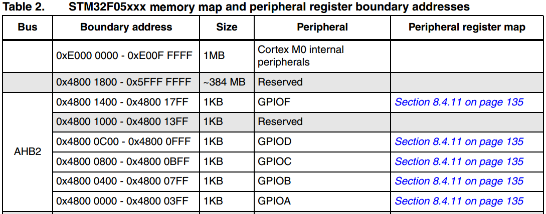
This means that at address 0x48000800 a structure starts of type GPIO_TypeDef.
And GPIOC is defined as a pointer to this structure:
As GPIOC is a pointer to a structure, we are able to access any member of this structure using the dereference operator. For instance, we can use the instruction
GPIOC->PUPDR = 0x00000000;
to write all zero’s to the PUPDR register (instead of using address 0x4800080C).
Accessing registers like this makes code very readable. One significant other advantage of this method is the portability of the main application code. By including another header file for a different microcontroller (vendor), the defined addresses will be different, but this is irrelevant to the application code.
This way of making the peripherals registers accessible in C is called the Cortex Microcontroller Software Interface Standard (CMSIS). CMSIS is a vendor-independent hardware abstraction layer for the Cortex-M processor series. The CMSIS enables consistent and simple software interfaces to the processor and the peripherals, simplifying software re-use, reducing the learning curve for new microcontroller developers and reducing the time to market for new devices.[1]
By default, all peripheral clocks are disabled to save power. This means the programmer must enable each peripheral clock within the Reset and Clock Control (RCC) register. GPIOC clock is enabled with the instruction:
RCC->AHBENR |= RCC_AHBENR_GPIOCEN;
Finally, lets take a look at the delay routine:
void delay(const int d)
{
volatile int i;
for(i=d; i>0; i--){ ; }
return;
}
|
When compiled with maximum optimization level (-O3), the for-loop in this delay function produces the following assembly instructions (as can be seen when the debugger is started):
Cycles required
0x080000E2 9000 STR r0,[sp,#0x00] 2
0x080000E4 2800 CMP r0,#0x00 1
0x080000E6 DD01 BLE 0x080000EC 1
0x080000E8 1E40 SUBS r0,r0,#1 1
0x080000EA E7FA B 0x080000E2 3
|
When we know the number of cycles for each instruction, the timing of one for-loop is calculated easily:
The number of cycles for each instruction can be found in the Cortex-M0 instruction set, for instance here:
We can conclude that this delay function requires 8 cycles for each for-loop.
The global variable SystemCoreClock is provided by the startup file system_stm32f0xx.c. Therefore, if we want a delay of approximately 1 second, the delay function should be called with a parameter of
By using this global variable SystemCoreclock, the code will be more portable across devices.
Assignment 1
So far we have seen how to use outputs. In a similar way inputs can be used.
Adapt the project blinky.uvprojx so that:
- when the blue USER Push button is not pressed, the delay time is ~ 1 sec.
- when the blue USER Push button is pressed, the delay time is ~ 0.1 sec.
Tips:
- The features of the STM32F0DISCOVERY board are described in the User Manual UM1525, which can be found on the STM32F0DISCOVERY website. In paragraph 4.9 is described which I/O pin is connected to the blue USER Push button.
- Remember to also enable this I/O pin’s peripheral clock!
Assignment 2
Use a breadboard and connect eight LED’s to PC0 to PC7.
Implement a LED chaser that changes direction when pressing the blue USER Push button.
Không có nhận xét nào:
Đăng nhận xét