Analog-to-Digital Convertor
The 12-bit ADC is a successive approximation analog-to-digital converter. It has up to 19 multiplexed channels allowing it to measure signals from 16 external and 3 internal sources. A/D conversion of the various channels can be performed in single, continuous, scan or discontinuous mode. The result of the ADC is stored in a left-aligned or right-aligned 16-bit data register.[1]
The ADC is explained using the following block diagram:

The ‘Input Selection & Scan Control’-block selects one of the multiplexed analog input channels ADC_IN[15:0] or the internal input channels VBAT, VREF and TS. This is done in single or continuous conversion mode and users may decide to scan upward (ADC_IN0 first) or backward (VBAT first).
Starting and stopping a sequence of conversions is controlled by the ‘Start & Stop Control’-block. A sequence of conversions may contain any number of channels between one and nineteen, which is configurable by the user.
Before starting one of the conversions in the sequence, the ADC needs to establish a direct connection between the voltage source to be measured and the embedded sampling capacitor of the ADC. This sampling time must be enough for the input voltage source to charge the sample and hold capacitor to the input voltage level. Having a programmable sampling time allows to trim the conversion speed according to the input resistance of the input voltage source. Starting and stopping can also be triggered by timers.
The ‘SAR ADC’-block implements the successive approximation hardware. An n-bit successive approximation ADC takes at least n successive steps to approximate the analog input to a digital representation.
The time between the start and the end of a conversion is determined by:
- the ADC clock, which determines the time of one cycle
- the number of cycles required for sampling, called the 'sample time'
- the number of cycles for successive approximation, depending on the resolution.
By default, the ADC is clocked with a dedicated 14 MHz internal oscillator.
The ‘Analog Watchdog’-block allows the application to detect if the input voltage goes outside the user-defined higher or lower thresholds. A status flag can be read or an interrupt can be generated.
Through the APB interface the conversion result can be transferred. This can be done by the Cortex-M0 core or the DMA controller.
This lesson has four examples to show how the ADC can be used. There is one μVision project with four different ADC targets:
- ADC Single Conversion
- ADC Continuous Conversion
- ADC Temperature Sensor
- ADC Window Watchdog
The following hardware setup is required for these examples:
An FT232RL Breakout Board (https://www.sparkfun.com/products/718) (or any other level shifter) is used to communicate with a terminal program (like PuTTYhttp://www.chiark.greenend.org.uk/~sgtatham/putty/download.html).
A potentiometer is connected to PC1, input channel 11 of ADC1. Use any value from 1 kΩ to 10 kΩ.
All example programs make use of several ‘helper’-functions, like a delay and USART setup. The functions are implemented in the file helper.c and are implemented as a utility, just like the stm32f0-discovery utility files, but are placed in the user folder.
All standard peripheral library files required for this project (9 in total) are added to the folder stm32f0-stdperiphlib.
Single conversion mode
Open the project associated with this lesson and select the target ADC Single Conversion. The goal of this project is to get an ADC sample from channel 11 (PC1), convert it to an ASCII-string and display it in a terminal program.
The first thing done in the main function is initializing the hardware available on the STM32F0Discovery Evaluation kit (LED’s and user pushbutton) with the utility functions provided in stm32f0_discovery.c, although they are not used in this program.
Then the USART is configured. Instead of doing this in the main routine, the function USART_Setup() is used. This function configures USART1 in default mode, except for a higher baud rate. USART1 will be configured with 115200, 8, n, 1. We will not look into the details of configuring the USART, as this has been done in lesson 3.
ADC1 is also configured using a function: ADC_Setup(). Let’s take a closer look at this function and how it enables us to use the ADC in single conversion mode. The peripheral driver library file of the ADC gives all the information on how to use the driver:
================================================================================
##### How to use this driver #####
================================================================================
[..]
(#) Enable the ADC interface clock using
RCC_APB2PeriphClockCmd(RCC_APB2Periph_ADC1, ENABLE);
(#) ADC pins configuration
(++) Enable the clock for the ADC GPIOs using the following function:
RCC_AHBPeriphClockCmd(RCC_AHBPeriph_GPIOx, ENABLE);
(++) Configure these ADC pins in analog mode using GPIO_Init();
(#) Configure the ADC conversion resolution, data alignment, external
trigger and edge, scan direction and Enable/Disable the continuous mode
using the ADC_Init() function.
(#) Activate the ADC peripheral using ADC_Cmd() function.
|
These steps are implemented in the function ADC_Setup():
/**
* @brief This function sets PC1 to analog mode, initializes and
* calibrates ADC1.
* @param None
* @retval None
*/
void ADC_Setup(void)
{
GPIO_InitTypeDef GPIO_InitStructure;
ADC_InitTypeDef ADC_InitStructure;
//(#) Enable the ADC interface clock using
// RCC_APB2PeriphClockCmd(RCC_APB2Periph_ADC1, ENABLE);
RCC_APB2PeriphClockCmd(RCC_APB2Periph_ADC1, ENABLE);
//(#) ADC pins configuration
// (++) Enable the clock for the ADC GPIOs using the following function:
// RCC_AHBPeriphClockCmd(RCC_AHBPeriph_GPIOx, ENABLE);
// (++) Configure these ADC pins in analog mode using GPIO_Init();
RCC_AHBPeriphClockCmd(RCC_AHBPeriph_GPIOC, ENABLE);
GPIO_InitStructure.GPIO_Pin = GPIO_Pin_1;
GPIO_InitStructure.GPIO_Mode = GPIO_Mode_AN;
GPIO_InitStructure.GPIO_PuPd = GPIO_PuPd_NOPULL ;
GPIO_Init(GPIOC, &GPIO_InitStructure);
//(#) Configure the ADC conversion resolution, data alignment, external
// trigger and edge, scan direction and Enable/Disable the continuous mode
// using the ADC_Init() function.
ADC_InitStructure.ADC_Resolution = ADC_Resolution_12b;
ADC_InitStructure.ADC_ContinuousConvMode = DISABLE;
ADC_InitStructure.ADC_ExternalTrigConvEdge = ADC_ExternalTrigConvEdge_None;
ADC_InitStructure.ADC_DataAlign = ADC_DataAlign_Right;
ADC_InitStructure.ADC_ScanDirection = ADC_ScanDirection_Upward;
ADC_Init(ADC1, &ADC_InitStructure);
// Calibrate ADC before enabling
ADC_GetCalibrationFactor(ADC1);
//(#) Activate the ADC peripheral using ADC_Cmd() function.
ADC_Cmd(ADC1, ENABLE);
// Wait until ADC enabled
while(ADC_GetFlagStatus(ADC1, ADC_FLAG_ADEN) == RESET);
}
|
Some things to notice are the following. We want to use ADC channel 11 which is connected to PORTC I/O-pin 1. We use a GPIO_InitTypeDef structure to configure this pin in analog mode. Notice that there is no need to set an Alternate Function.
With an ADC_InitTypeDef the ADC1 is configured. This example shows the single conversion mode, therefore ContinuousConvMode is disabled and there will be no external trigger.
The result will be a 12-bit right aligned integer and the four most significant bits will read logic 0:
15
|
14
|
13
|
12
|
11
|
10
|
9
|
8
|
7
|
6
|
5
|
4
|
3
|
2
|
1
|
0
|
0
|
0
|
0
|
0
|
n
|
n
|
n
|
n
|
n
|
n
|
n
|
n
|
n
|
n
|
n
|
n
|
If we want a full excursion of the ADC result (from 0 to 4095), the ADC must be calibrated. The peripheral driver library supplies a function to do this, which must be called before activating the ADC peripheral:
ADC_GetCalibrationFactor(ADC1);
Finally, after the ADC is enabled, we wait for the ADC to be ready by checking the ADC Enable flag:
while(ADC_GetFlagStatus(ADC1, ADC_FLAG_ADEN) == RESET);
After calling the function ADC_Setup() in the main-loop, the channels that must be part of the conversion sequence must be configured. Each channel can be set with a dedicated sampling time and the peripheral driver library supplies a function to configure this:
ADC_ChannelConfig(ADC1, ADC_Channel_11, ADC_SampleTime_239_5Cycles);
We can now calculate the time required for one AD-conversion of channel 11.
The default ADC clock is 14 MHz, so one clock cycle takes:
(1)
|
According to paragraph 13.4.6 in the Reference Manual RM0091 the total conversion time is calculated with:
(2)
|
In the example code the sampling time is configured to 239,5 cycles. The SAR time equals 12,5 cycles (because we use 12 bit resolution, see also table 33 in RM0091). This makes a total conversion time of 18 μs for one sample.
Getting an analog value is initiated with the function:
ADC_StartOfConversion(ADC1);
This starts a sequence of conversions for all selected channels. With the following line of code we wait until a single conversion is complete:
while(ADC_GetFlagStatus(ADC1, ADC_FLAG_EOC) == RESET){;}
After that the conversion result is read into a 16-bit unsigned integer with:
adc = ADC_GetConversionValue(ADC1);
In this example there is only one channel configured, so after the first conversion is ready we know the conversion sequence is ready too. There is also a status flag to check if the total conversion sequence is ready:
while(ADC_GetFlagStatus(ADC1, ADC_FLAG_EOSEQ) == RESET){;}
Assignments
When the ADC is clocked at 14 MHz, what is the fastest total conversion time that can be realized with 12-bit precision? And with 6-bit precision?
What is the meaning of the OVR flag in the ADC_ISR register?
Continuous conversion mode
Open the project associated with this lesson and select the target ADC Continuous Conversion. The goal of this project is to get an ADC sample from channel 11 (PC1), convert it to an ASCII-string and display it in a terminal program.
This mode is very similar to the single conversion mode discussed before. Instead of starting each conversion sequence, conversion sequences are automatically restarted.
Therefore the function ADC_Setup() is pretty much equal to the single conversion mode example, except that ContinuousConvMode is enabled:
ADC_InitStructure.ADC_ContinuousConvMode = ENABLE;
|
Then in the main routine, the channel(s) must be configured and the first conversion needs to be started. In the main-loop we simply get the latest conversion result with the function:
adc = ADC_GetConversionValue(ADC1);
Temperature sensor
Open the project associated with this lesson and select the target ADC Temperature Sensor.
The goal of this project is to get an ADC sample from the internal temperature sensor, calculate this to degrees Celsius, convert this to an ASCII-string and display it in a terminal program.
The temperature sensor can be used to measure the junction temperature (TJ) of the device. The temperature sensor is internally connected to the ADC1_IN16 input channel which is used to convert the sensor’s output voltage to a digital value. The sampling time for the temperature sensor’s analog input must be greater than 17,1 μs. The temperature sensor output voltage changes linearly with temperature. The internal temperature sensor is more suitable for applications that detect temperature variations instead of absolute temperatures.
Using the temperature sensor in an application is very similar to the examples seen before. Instead of having an external channel activated, we only need to activate internal channel 16. In the function ADC_Setup() the initialisation of the GPIO can be omitted. In this example, the ADC is used in continuous mode.
The peripheral driver library describes how to use the Temperature sensor:
/** @defgroup ADC_Group4 Temperature Sensor, Vrefint and Vbat management functions
* @brief Temperature Sensor, Vrefint and Vbat management functions
*
@verbatim
===============================================================================
##### Temperature Sensor, Vrefint and Vbat management function #####
===============================================================================
[..] This section provides a function allowing to enable/disable the internal
connections between the ADC and the Temperature Sensor, the Vrefint and
Vbat source.
[..] A typical configuration to get the Temperature sensor, Vrefint and Vbat
channels voltages is done following these steps :
(#) Enable the internal connection of Temperature sensor, Vrefint or Vbat
sources with the ADC channels using ADC_TempSensorCmd(),
ADC_VrefintCmd() or ADC_VbatCmd() functions.
(#) select the ADC_Channel_16(Temperature sensor), ADC_Channel_17(Vrefint)
or ADC_Channel_18(Voltage battery) using ADC_ChannelConfig() function
(#) Get the voltage values, using ADC_GetConversionValue() function
@endverbatim
* @{
*/
|
In the file main3.c these steps are implemented after the function ADC_Setup() has been called:
int main(void)
{
uint16_t adc, temperature;
char str[10];
// Configure LED3 and LED4 on STM32F0-Discovery
STM_EVAL_LEDInit(LED3);
STM_EVAL_LEDInit(LED4);
// Initialize User Button on STM32F0-Discovery
STM_EVAL_PBInit(BUTTON_USER, BUTTON_MODE_GPIO);
USART_Setup();
USART_Clearscreen();
USART_Putstr("Lesson 5: ADC Temperature Sensor\n");
ADC_Setup();
//(#) Enable the internal connection of Temperature sensor, Vrefint or Vbat
// sources with the ADC channels using ADC_TempSensorCmd(), ADC_VrefintCmd()
// or ADC_VbatCmd() functions.
ADC_TempSensorCmd(ENABLE);
//(#) select the ADC_Channel_16(Temperature sensor), ADC_Channel_17(Vrefint)
// or ADC_Channel_18(Voltage battery) using ADC_ChannelConfig() function
ADC_ChannelConfig(ADC1, ADC_Channel_16, ADC_SampleTime_28_5Cycles);
// Start the first conversion
ADC_StartOfConversion(ADC1);
while(1)
{
// Delay ~0.2 sec.
Delay(SystemCoreClock/8/5);
//(#) Get the voltage values, using ADC_GetConversionValue() function
adc = ADC_GetConversionValue(ADC1);
// Calculate corresponding voltage level
// V25 = (4095 * 1.43V) / 3V = 1952
// Avg_Slope = 4.3mV / (3V / 4095) = 5,8695 ~ 6
temperature = ((1952 - adc) / 6) + 25;
// Output the values
USART_Putstr("Temperature: ");
USART_itoa(temperature, str);
USART_Putstr(str);
USART_Putstr(" degrees Celcius\r");
}
}
|
With the ADC result from the function ADC_GetConversionValue() we can calculate the temperature in degrees Celsius. The Reference Manual RM0091 describes in paragraph 12.9 how to calculate the temperature in degrees Celsius:
(3)
|
The Datasheet DS8668 provides the characteristics of the temperature sensor:
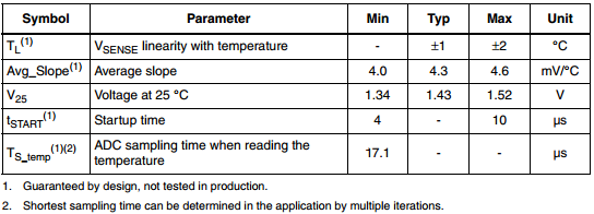
With this information, we can calculate the temperature easily. Let’s avoid floating point calculations, because the take much more time and code space then fixed point calculations. So we transfer the Typical values from the table above to the ‘digital’ domain.
(4)
|
(5)
|
So the temperature in degrees Celsius is:
(6)
|
Assignment
Change this example so it reads from two channels: the temperature sensor and external channel 11. The terminal program displays both values.
Window watchdog
Open the project associated with this lesson and select the target ADC Window Watchdog.
The goal of this project is to get an ADC sample from channel 11 (PC1), convert it to an ASCII-string and display it in a terminal program. Besides that, the blue LED goes on when the analog input value drops below 0,73 V or rises above 2,2 V.
In this example ADC1 is initialized in continuous conversion mode with the function ADC_Setup(). Besides that, the Window Watchdog is initialized with the function ADC_WindowWatchdogSetup(). And again, the peripheral driver library tells how to:
/** @defgroup ADC_Group3 Analog Watchdog configuration functions
* @brief Analog Watchdog configuration functions
*
@verbatim
===============================================================================
##### Analog Watchdog configuration functions #####
===============================================================================
[..] This section provides functions allowing to configure the Analog Watchdog
(AWD) feature in the ADC.
[..] A typical configuration Analog Watchdog is done following these steps :
(#) the ADC guarded channel(s) is (are) selected using the
ADC_AnalogWatchdogSingleChannelConfig() function.
(#) The Analog watchdog lower and higher threshold are configured using
the ADC_AnalogWatchdogThresholdsConfig() function.
(#) The Analog watchdog is enabled and configured to enable the check, on
one or more channels, using the ADC_AnalogWatchdogCmd() function.
(#) Enable the analog watchdog on the selected channel using
ADC_AnalogWatchdogSingleChannelCmd() function
@endverbatim
* @{
*/
|
These steps are implemented in the function ADC_WindowWatchdogSetup():
void ADC_WindowWatchdogSetup(void)
{
NVIC_InitTypeDef NVIC_InitStructure;
//(#) the ADC guarded channel(s) is (are) selected using the
// ADC_AnalogWatchdogSingleChannelConfig() function.
ADC_AnalogWatchdogSingleChannelConfig(ADC1, ADC_AnalogWatchdog_Channel_11);
//(#) The Analog watchdog lower and higher threshold are configured using the
// ADC_AnalogWatchdogThresholdsConfig() function.
ADC_AnalogWatchdogThresholdsConfig(ADC1, 3000, 1000);
//(#) The Analog watchdog is enabled and configured to enable the check, on one
// or more channels, using the ADC_AnalogWatchdogCmd() function.
ADC_AnalogWatchdogCmd(ADC1, ENABLE);
//(#) Enable the analog watchdog on the selected channel using
// ADC_AnalogWatchdogSingleChannelCmd() function
ADC_AnalogWatchdogSingleChannelCmd(ADC1, ENABLE);
// Enable ADC1 interrupts
NVIC_InitStructure.NVIC_IRQChannel = ADC1_COMP_IRQn;
NVIC_InitStructure.NVIC_IRQChannelPriority = 0;
NVIC_InitStructure.NVIC_IRQChannelCmd = ENABLE;
NVIC_Init(&NVIC_InitStructure);
// Enable Watchdog interrupt
ADC_ITConfig(ADC1, ADC_IT_AWD, ENABLE);
}
|
The upper- and lower thresholds are calculated with:
(7)
|
(8)
|
We also want an interrupt to be triggered when the watchdog detects an input value above the upper threshold or below the lower threshold. We therefore initialize the global ADC1-and-Comparator interrupt in the NVIC. After that the watchdog interrupt is enabled with the driver function ADC_ITConfig().
In the file stm32f0xx_it.c the ADC1_and_Comparator interrupt handler has been added. It first checks to make sure the ADC window watchdog triggered the interrupt handler and then turns on the blue LED:
/**
* @brief This function handles ADC1 and COMP global interrupt request.
* @param None
* @retval None
*/
void ADC1_COMP_IRQHandler(void)
{
if(ADC_GetITStatus(ADC1, ADC_IT_AWD) != RESET)
{
ADC_ClearITPendingBit(ADC1, ADC_IT_AWD);
// Turn on Window Watchdog indicator
STM_EVAL_LEDOn(LED4);
}
}
|
Assignment
Use the watchdog to generate an interrupt if the device temperature drops below 15 °C or rises above 30 °C.
Digital-to-Analog Convertor
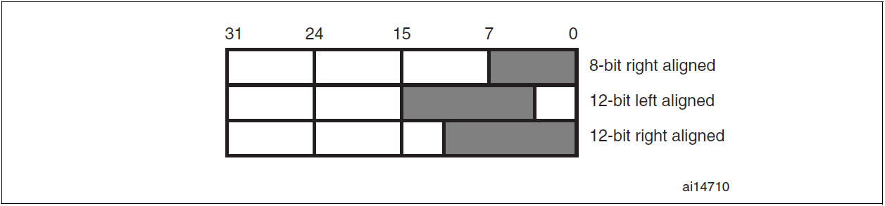
The DAC module is a 12-bit, voltage output digital-to-analog converter. The DAC can be configured in 8- or 12-bit mode and may be used in conjunction with the DMA controller. In 12-bit mode, the data could be left- or right-aligned.[2]
The DAC is explained with it’s block diagram:
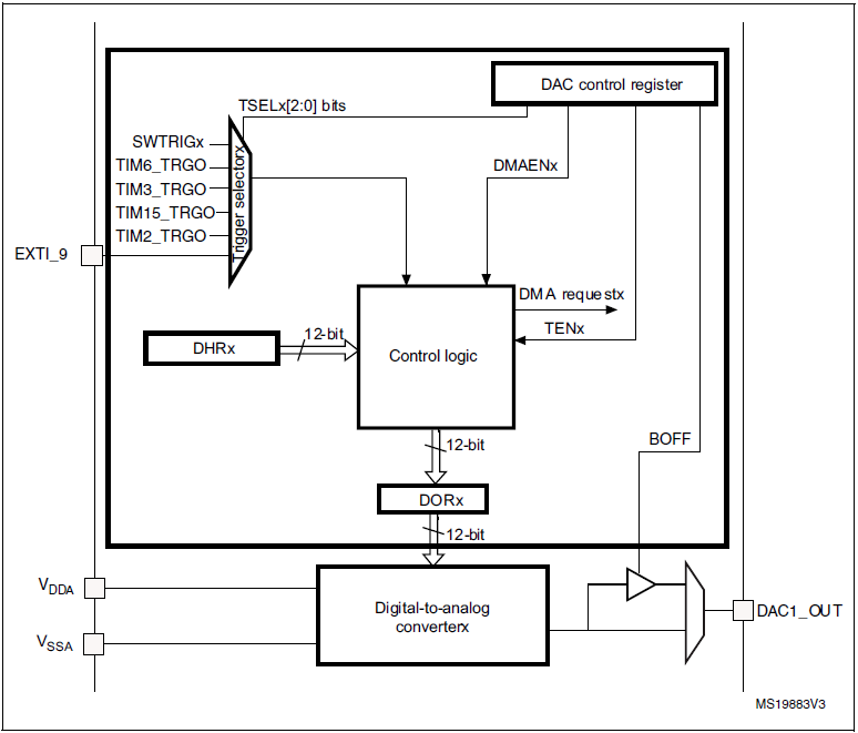
The digital value cannot be written directly to the `Digital-to-analog converterx`-block, instead a Data Holding Register (DHRx) is used. The DHRx register is then loaded into the Data Output Register (DORx) automatically, by software trigger or by an external event trigger like a timer. The ‘Control Logic’-block controls these signals and settings are made in the ‘DAC control register’-block.
After a trigger, the `Digital-to-analog converterx`-block converts the digital data in a linear fashion to an analog value between VDDA and VSSA. This voltage is calculated with the following formula, assuming 12-bit precision and VSSA equals GND:
(9)
|
It should be noted however that paragraph 6.3.16 of the Datasheet DS8668 provides accurate information on the DAC minimum and maximum output levels:


Notice that disabling the output buffer with the BOFF-bit in the control register has significant effect on the output ranges. The advantage however of using an output buffer is that output impedance is reduced so external loads can be driven directly (without for instance the need for an external opamp).
The example projects associated with the DAC use the following hardware setup:
The example projects will discuss two modes of operation: Single mode and external triggering with a timer.
Single mode
Open the project associated with this lesson and select the target DAC Single Mode. The goal of this project is to generate a pulse on the LED connected to DAC1_OUT (PA4).
First we take a look at the peripheral driver library, so we know how to use the driver:
##### How to use this driver #####
===============================================================================
[..]
(+) Enable DAC APB1 clock to get write access to DAC registers
using RCC_APB1PeriphClockCmd(RCC_APB1Periph_DAC, ENABLE)
(+) Configure DAC_OUT1 (DAC_OUT1: PA4) in analog mode
using GPIO_Init() function
(+) Configure the DAC channel using DAC_Init()
(+) Enable the DAC channel using DAC_Cmd()
|
These steps are implemented in the function DAC_Setup():
/**
* @brief This function sets PA4 to analog mode and initializes
* DAC1.
* @param None
* @retval None
*/
void DAC_Setup(void)
{
GPIO_InitTypeDef GPIO_InitStructure;
DAC_InitTypeDef DAC_InitStructure;
//(+) Enable DAC APB1 clock to get write access to DAC registers
// using RCC_APB1PeriphClockCmd(RCC_APB1Periph_DAC, ENABLE)
RCC_APB1PeriphClockCmd(RCC_APB1Periph_DAC, ENABLE);
//(+) Configure DAC_OUT1 (DAC_OUT1: PA4) in analog mode
// using GPIO_Init() function
GPIO_InitStructure.GPIO_Pin = GPIO_Pin_4;
GPIO_InitStructure.GPIO_Mode = GPIO_Mode_AN;
GPIO_InitStructure.GPIO_PuPd = GPIO_PuPd_NOPULL;
GPIO_Init(GPIOA, &GPIO_InitStructure);
//(+) Configure the DAC channel using DAC_Init()
DAC_InitStructure.DAC_Trigger = DAC_Trigger_None;
DAC_InitStructure.DAC_OutputBuffer = DAC_OutputBuffer_Enable;
DAC_Init(DAC_Channel_1, &DAC_InitStructure);
//(+) Enable the DAC channel using DAC_Cmd()
DAC_Cmd(DAC_Channel_1, ENABLE);
}
|
In single mode there is no trigger required and when data is written into the DHRx, it will automatically be written to the DORx.
After the DAC has been setup, the main routine can start writing data to the DHRx. The peripheral driver library has the following function to do this:
DAC_SetChannel1Data(DAC_Align_12b_R, i);
The first parameter describes the alignment of the data.There are three options:
LED’s have a threshold voltage called ULED before they conduct current. This means that the output voltage of the DAC should at least exceed this voltage before the LED will light up. When ULED = 1,8 V, then the digital value written to the DAC needs to be at least:
(10)
|
So any value between 0 and 2457 will not make the LED light up!
In the main loop you see this range excluded from both for-loops. A delay of 1 ms is used so one for loop takes approximately 1683 ms.
Assignment
When Vdd = 3 V and ULED = 1,8 V, what is the maximum voltage over the resistor when the DAC output buffer is enabled?
What value for the resistor should be chosen if the maximum current should not exceed 20 mA?
External trigger
Open the project associated with this lesson and select the target DAC External Trigger. The goal of this project is to generate a pulse on the LED connected to DAC1_OUT (PA4). The changes of the pulse are made visible only once every second.
In the DAC_Setup() function an external trigger source is selected: TIM3. Also in this function TIM3 is initialized in exactly the same way as seen in lesson 4. The timebase is set to 1 second and the Trigger Output (TRGO) is triggered every time the Update event (1 second has expired) takes place.
/**
* @brief This function sets PA4 to analog mode and initializes
* DAC1. The DAC will be triggered externally by the TIM3 TRGO
* command. TIM3 is initialzed to generate TRGO trigger every second.
* @param None
* @retval None
*/
void DAC_Setup(void)
{
GPIO_InitTypeDef GPIO_InitStructure;
DAC_InitTypeDef DAC_InitStructure;
TIM_TimeBaseInitTypeDef TIM_TimeBaseStructure;
//(+) Enable DAC APB1 clock to get write access to DAC registers
// using RCC_APB1PeriphClockCmd(RCC_APB1Periph_DAC, ENABLE)
RCC_APB1PeriphClockCmd(RCC_APB1Periph_DAC, ENABLE);
//(+) Configure DAC_OUT1 (DAC_OUT1: PA4) in analog mode
// using GPIO_Init() function
GPIO_InitStructure.GPIO_Pin = GPIO_Pin_4;
GPIO_InitStructure.GPIO_Mode = GPIO_Mode_AN;
GPIO_InitStructure.GPIO_PuPd = GPIO_PuPd_NOPULL;
GPIO_Init(GPIOA, &GPIO_InitStructure);
//(+) Configure the DAC channel using DAC_Init()
DAC_InitStructure.DAC_Trigger = DAC_Trigger_T3_TRGO;
DAC_InitStructure.DAC_OutputBuffer = DAC_OutputBuffer_Enable;
DAC_Init(DAC_Channel_1, &DAC_InitStructure);
//(+) Enable the DAC channel using DAC_Cmd()
DAC_Cmd(DAC_Channel_1, ENABLE);
//(#) Enable TIM clock using
// RCC_APBxPeriphClockCmd(RCC_APBxPeriph_TIMx, ENABLE) function.
RCC_APB1PeriphClockCmd(RCC_APB1Periph_TIM3, ENABLE);
//(#) Fill the TIM_TimeBaseInitStruct with the desired parameters.
TIM_TimeBaseStructInit(&TIM_TimeBaseStructure);
TIM_TimeBaseStructure.TIM_CounterMode = TIM_CounterMode_Up;
TIM_TimeBaseStructure.TIM_Period = 1000-1;
TIM_TimeBaseStructure.TIM_Prescaler = (uint16_t)((SystemCoreClock / 1000) - 1);
//(#) Call TIM_TimeBaseInit(TIMx, &TIM_TimeBaseInitStruct) to configure
// the Time Base unit with the corresponding configuration.
TIM_TimeBaseInit(TIM3, &TIM_TimeBaseStructure);
// TIM3 TRGO selection
TIM_SelectOutputTrigger(TIM3, TIM_TRGOSource_Update);
//(#) Call the TIM_Cmd(ENABLE) function to enable the TIM counter.
TIM_Cmd(TIM3, ENABLE);
}
|
The main routine does exactly the same as the single mode example. The contents of the DHRx is however written once per second to the DORx.
Assignment
Change this example to generate a sine wave with a frequency of 1 kHz. Make use of the following lookup table:
const uint16_t sine12bit_lut[32] = {
2047, 2447, 2831, 3185, 3498, 3750, 3939, 4056,
4095, 4056, 3939, 3750, 3495, 3185, 2831, 2447,
2047, 1647, 1263, 909, 599, 344, 155, 38,
0, 38, 155, 344, 599, 909, 1263, 1647};
Use an oscilloscope to make the generated wave visible.
TIP: Read from DORx in the main loop to determine if the next value can be written to the DHRx. Look for a function in the peripheral driver library to read from DORx!
Trả lờiXóaI just want to say thank you for sharing this post, it was really awesome and very informative. Thank you.
OET Coaching for Nurses in Melbourne
ADC Coaching for Dentist in Melbourne
AMC Coaching for Doctors in Melbourne
OET Coaching in Adelaide
can you fix you picture. I want to see result. tks!!!
Trả lờiXóaharikasın
Trả lờiXóa